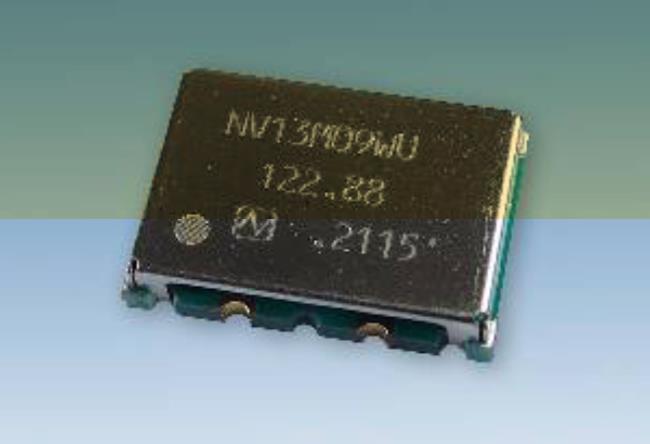
Nihon Dempa Kogyo Co., Ltd. has developed a compact, low-profile, ultra-low phase noise VCXO ( Ultra Low Noise VCXO of 13.8×9.2×2.8mm in size).Sample shipments will start from June 2021.
The 5th-generation mobile communication systems (5G) service has started in Japan. In the future, the use of 5G communications in autonomous driving and the widespread use of IoTs are expected to further increase the amount of communications, and it is expected that system will become faster and more responsive (with lower delays).
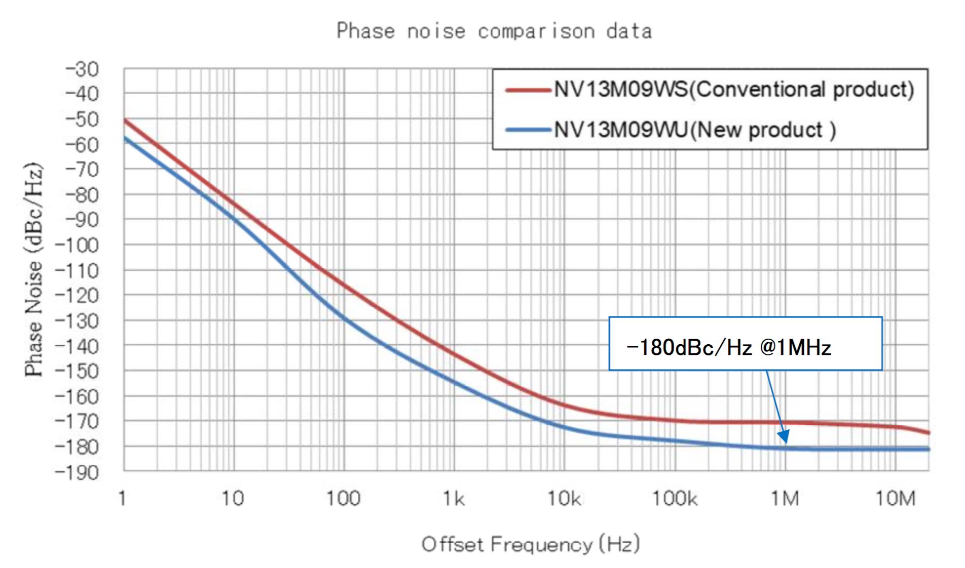
In order to ensure these communications qualities, a compact crystal oscillator with good phase noise characteristics is required particularly for the synchronization circuit of the local oscillator and the control unit of the radio section in the base station. To meet this need, we have developed a VCXO that realizes a floor noise of-180 dBc/Hz.
In particular, this can contribute to 5G base station applications < RU/BBU (CU/DU) > (*2).
Using our crystal unit design using high-quality synthetic quartz crystal and low-phase noise circuit design, we have achived floor noise of Typ.-178 dBc/Hz (offset frequency: 100kHz) and Typ.-180 dBc/Hz (offset frequency: 1MHz or higher). Compared with our conventional ultra-low phase noise VCXO (NV13M09WS), the floor noise has improved to 9-12dB over 100kHz, which is the highest level in the industry.
Sample shipments of this product are scheduled to begin in June 2021, and mass production will begin in November 2021. We plan to expand our product lineup by expanding the range of output frequencies and supporting CMOS output.
We will continue to provide highly reliable, high-precision products required in 5G era, and contribute to the realization of a safe, secure, and comfortable society through our quartz device and crystal based equipment business.
| Model | NV13M09WU |
| External Dimensions | 13.8 × 9.2 × 2.8 mm |
| Frequency Range | 100 to 156.25 MHz |
| Standard Frequency | 100 MHz, 122.88 MHz |
| Control Voltage Range | 5 V+/-5 % |
| Control Voltage Range | 2.5 V+/-2.5 V |
| Operating Temperature Range | -40 to +85 °C |
| Current Consumption | Max. 35 mA |
| Overall Frequency Tolerance (*3) | Max. +/-40 × 10-6 |
| Output Level, Load | Sine wave, Min.10 dBm, 50Ω |
| Absolute Pull Range (APR) (*4) | Min. +/-5 × 10-6 |
| Phase Noise (@100 MHz) | Typ. -90 dBc/Hz @ 10 Hz |
| Typ. -130 dBc/Hz @ 100 Hz | |
| Typ. -154 dBc/Hz @ 1 kHz | |
| Typ. -172 dBc/Hz @ 10 kHz | |
| Typ. -178 dBc/Hz @ 100 kHz | |
| Typ. -180 dBc/Hz @ 1 MHz | |
| Typ. -181 dBc/Hz @ 10 MHz | |
| Phase Jitter (@100 MHz) | Typ. 9 fs (12 kHz to 20 MHz) |
*1:Based on our investigation in April 2021
*2:RU(Radio Unit :Radio satellite station) BBU(Base Band Unit:Baseband portion)
CU(Central Unit:Aggregate Nodes) DU(Distributed Unit:Distributed node) *3:Overall Frequency Tolerance
= (Frequency Tolerance) + (Frequency/Temperature Characteristics) + (Frequency/Voltage Coefficient) + (Long-term Frequency Stability (10 years))
*4:Absolute Pull Range (APR:Absolute Pull Range)
= Frequency Pulling Range-Overall Frequency Tolerance