
Nihon Dempa Kogyo Co., Ltd. has developed a low-phase jitter differential-output crystal oscillator(product size: 3.2 x 2.5 x 1.0mm) with the industry’s highest level (*1). Sample shipments will begin in February 2020.
In recent years, there has been a growing need for further low-jitter reference clocks to improve communication performance in high-speed mobile communications such as 5G and LTE, and in serial communications such as SONET/SDH, 10Gbit/Ethernet, SATA, and PCI-Express, both at higher speeds and at larger capacities.
If the jitter is large, it may interfere with adjacent signals and cause noise and communication performance deterioration.
To meet these needs, in June 2018 we released a LVDS differential-output crystal oscillator with phase jitter reduced to 57fs (at 156. 25MHz). After that, we developed a high-frequency fundamental-wave crystal unit using photolithography technology and a low-noise differential-oscilla tion IC. As a result, we succeeded in developing a LVDS, PECL differential-output crystal oscillator with lower noise than before. LVDS differential output crystal oscillator has a phase jitter of 47fs typ. (*1) which is a 10fs typ. reduction compared to the conventional product.
In the future, we will use this technology to gradually expand our lineup of products to other differential output methods, HCSL output, to meet the needs of our customers.
(*1) : Phase Jitter: 47fs typ. Oscillating Frequency: 156.25MHz, Power Supply Voltage 3.3V, 12kHz to 20MHz
[Sample/Mass production]Sample shipments are scheduled to begin in February 2020, and mass production is scheduled in September 2020.
[Product Characteristics]| NP3225SAB | NP3225SBB | |
| Product Appearance | 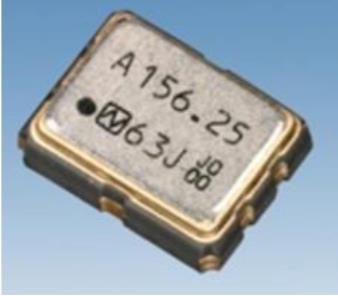 |
 |
| Size | 3.2 x 2.5 x Max.1.0 mm | |
| Nominal Frequency Range | 100MHz to 200MHz | |
| Output response | LVPECL | LVDS |
| Operating Temperature Range | -40deg.C to +85deg.C (Option : -40deg.C to +105deg.C) | |
| Overall Frequency Tolerance | Max.+/- 50 x 10-6 | |
| Power Supply Voltage [VCC] | +2.5V/+3.3V | |
| Period jitter (1σ) | Typ.0.9ps (156.25MHz) | Typ.0.8ps (156.25MHz) |
| Phase jitter (12kHz to 20MHz) |
Typ.42fs (156.25MHz) Typ.49fs (125MHz) Typ.57fs (100MHz) | Typ.47fs (156.25MHz) Typ.59fs (125MHz) Typ.80fs (100MHz) |
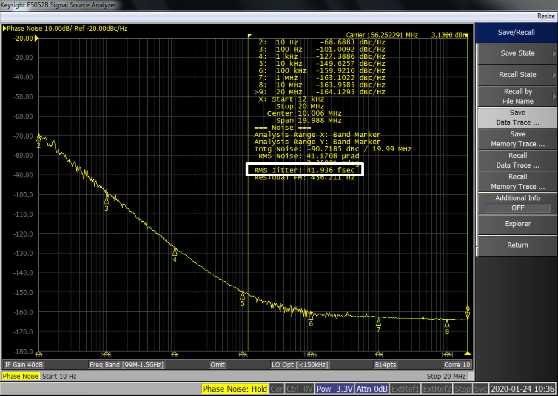
Condition: Nominal frequency 156.25MHz, LVPECL output, power supply voltage [VCC] +3.3V, temperature +25deg.C
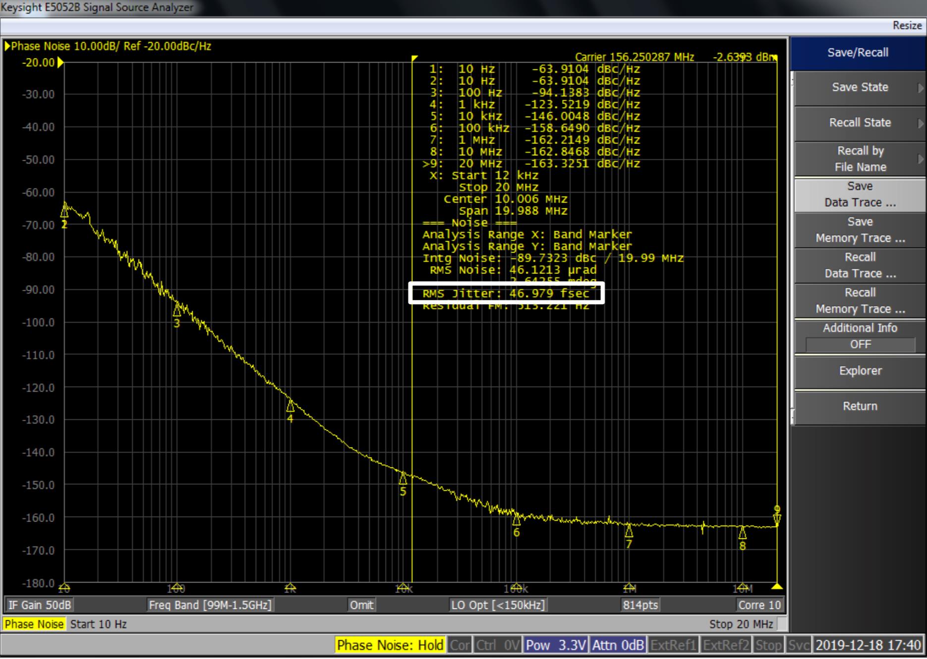
Condition: Nominal frequency 156.25MHz, LVDS output, power supply voltage [VCC] +3.3V, temperature +25deg.C
For more information on the product, please contact:
[Contact Info] e-Mail : [email protected]